|
False-colored scanning electron microscopy picture of a microbridge (adapted from Ref. [1]. Copyright Wiley-VCH Verlag GmbH & Co. KGaA. Reproduced with permission.) |
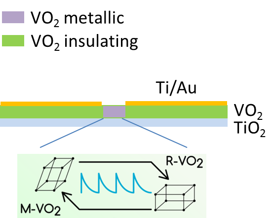
This device has been firstly realized in collaboration with TU-DELFT (The Netherlands).
It consists of a 100 µm × 5 µm free-standing microbridge made of a TiO2 (23 nm) /VO2 (90 nm) crystalline bilayer deposited by PLD on a MgO(100) substrate. The device is realized by patterning a resist mask by e-beam lithography, etching the bilayer by Argon milling and then making it freestanding using a 8.5% H3PO4 solution in water. Ti/Au electrodes (50 nm thick) partially cover the structure and are made by lift-off technique and deposited by electron beam evaporation. |
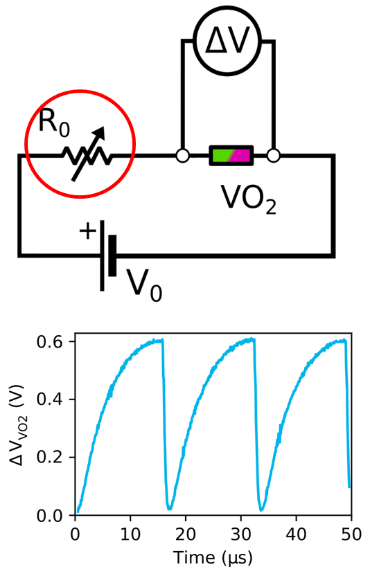
Electrical oscillationsThe reason for leaving a small gap of VO2 uncovered by the Ti/Au ohmic contacts relies on the fact that in this configuration the electro-thermal heating from Joule effect occurs mainly in the VO2 gap region, where the electrical resistance is higher. A voltage bias applied to contacts can thus produce a temperature increase sufficient to trigger the phase transition, making the VO2 gap region to change from the low temperature monoclinic phase to the high temperature rutile-type phase. This region is small if compared to the bridge length, thus the change of stress over the whole bridge is small as well and the resonance frequency of the mechanical structure is practically unaffected by the volume change of the VO2 within the gap region. |
|
|
By proper tuning the applied DC voltage and the value of a resistor place in series with the microbridge it is possible to onset a periodic phase transition of the VO2 gap region that can be easily detected by an oscillating current. The phenomenon of spontaneous oscillations is a general consequence of non-linear dynamics and the possibilty to onset electro-thermal oscillations in VO2 compounds is known since long time [4]. This effect is due to electro-thermal instabilities of the system under its sharp change of electrical resistance that takes place at the phase transition temperature. The electrical current heats up the structure by Joule effect and the resistance rapidly achieves a lower value, decreasing in its turn the amount of Joule heating and making the VO2 gap setting again on its low-temperature monoclinic VO2 phase. This periodic process is self-sustained only for selected values of the series resistor and applied DC voltages. |
Scheme of the circuit used for setting periodic electrical oscillation on the microbridge. A bias voltage V0 and an external resistor R0 are tuned to achieve electrical oscillations across the VO2 devices, detected as a periodic voltage waveform across its contacts (ΔVVO2) |
| This video shows the voltage drop across a VO2 microbridge following a step voltage bias of different magnitudes. At low voltages, the RC response of the voltage divider is measured, where C is the parasitic capacitance of the whole circuit. By increasing the voltage, the VO2 element is progressively heated and non-linear response appears due to its change of electrical resistance. Electrical oscillations appear in a particular window of bias voltage values and, if the voltage bias is too high, the VO2 metallic phase is maintained permanently. | |
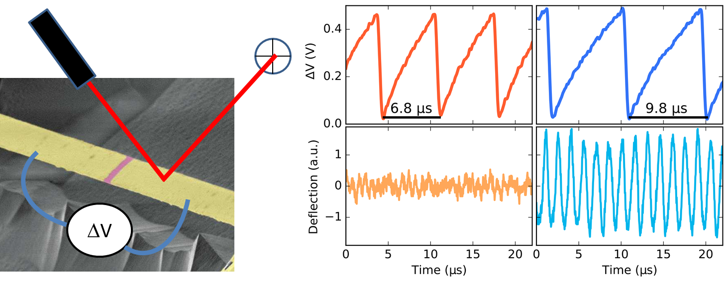
Mechanical excitationThe periodic VO2 phase transitions perturb the whole microbridge whose movement is amplified when the frequency of the electrical oscillation, or one of its harmonics components, is matched with one of the mechanical eigenfrequencies of the freestanding device. Tuning the applied DC voltage changes the electrical oscillations frequency and allows to ‘turn on’ a selected vibrational mode of the device (multimode excitation). |
|
|
Coupling electrical oscillation to mechanical motion. If the oscillating electrical signal (and its high-order harmonics) is not matched with the frequency of the mechanical modes, no significant movement is detected (left orange plot). When this occurs the flexural motion is amplified and easily observed by optical lever technique (right blue plot). These traces were acquired by keeping a constant V0 = 2 V and R0 in the 10–20 kΩ range. (adapted from ref. [1]. Copyright Wiley-VCH Verlag GmbH & Co. KGaA. Reproduced with permission.) |
|
|
The VO2 gap region thus works as a micrometer size engine that powers the oscillations of a bigger mechanical structure. All this is possible without using any external RF bias. This approach opens perspectives for realizing resonating micro-actuators powered using a simple DC voltage source. By controlling the domain size of VO2, this approach can be scalable to arrays of nanometric devices. Engineered VO2 gap regions can be used to power oscillatory motions of complex microstructures with potential applications in the fields of nano/micro robotic (i.e. locomotion), microfluidics or to power mechanical sensors at resonance. The research on these kinds of devices is underway and take advantages of using VO2 films with controlled domain size and crystalline orientation. This is made possible due to heteroepitaxial grow techniques. For further readings > [1] Selective High-Frequency Mechanical Actuation Driven by the VO2 Electronic Instability Manca N, Pellegrino L, Kanki T, Venstra W J, Mattoni G, Higuchi Y, Tanaka H, Caviglia A D and Marré D Adv. Mater. 1701618 (2017) [2] VO2: A Phase Change Material for Micromechanics Manca N, Pellegrino L, Kanki T, Venstra W, Mattoni G, Higuchi Y, Tanaka H, Caviglia A and Marré D Proceedings 1 294 doi:10.3390/proceedings1040294 (2017) [3] VO2: a material for high-performance micro/nanoactuators Manca N, Pellegrino L, Kanki T, Venstra W, Mattoni G, Higuchi Y, Tanaka H, Caviglia A and Marré D Proceeding Actuators 2018, Bremen [4] New oscillation phenomena in VO2 crystals Y. Taketa, F. Kato, M. Nitta, and M. Haradome, Appl. Phys. Lett. 27, 212 (1975) |
|